
UA launches semiconductor cleanroom, virtual reality lab
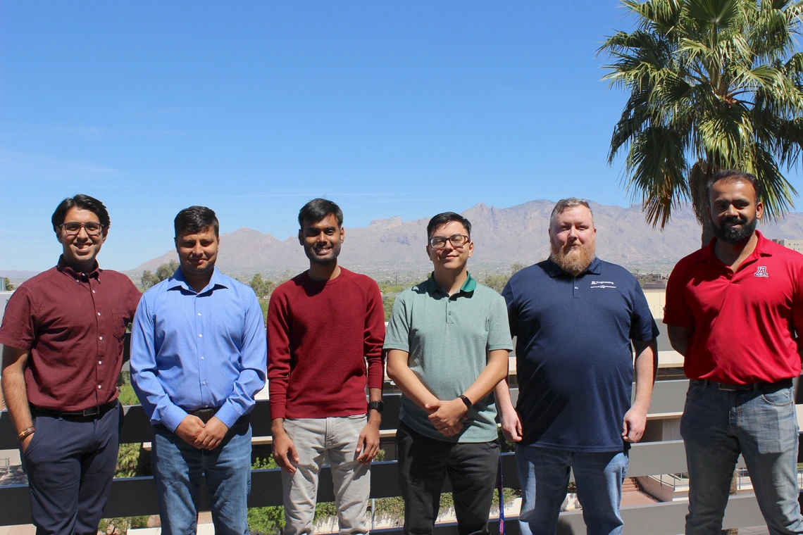
(From left) Soheil Salehi, Sujan Ghimire, Veeramani Pugazhenthi, John Martin Encinas, Josh Dean and Pratik Satam bring semiconductor education into the virtual realm with a digital twin of the University of Arizona’s cleanroom.
University, government and industry leaders unveiled the Office of Research and Partnerships' Nano Fabrication Center semiconductor cleanroom with a ribbon-cutting ceremony on Feb. 17.
Located in the Electrical and Computer Engineering Building, the cleanroom prepares students for Arizona’s booming tech sector while supporting faculty research and industry collaboration on chip fabrication, optical devices and quantum computing systems.
Next door, undergraduates tap into streamlined training with Apple Vision Pro and Meta Quest 3 headsets in the virtual reality lab, where up to 18 students can explore digital twins of the cleanroom and its equipment.
Inside the lab

Sujan Ghimire (left) helps a high school student with the VR headset.
ECE assistant professors Pratik Satam, Soheil Salehi and Ehsan Azimi led the development of the VR lab’s training resources.
At the ribbon-cutting, attendees toured a digital twin of the cleanroom – a virtual model that replicates its physical space and equipment – designed collaboratively by Satam’s and Salehi’s students John Martin Encinas, Josh Dean, Sujan Ghimire and Veeramani Pugazhenthi.
“The digital twin gives students a chance to interact with complex nanofabrication equipment before they ever set foot in the cleanroom,” Satam said.
The team used photographs and scans to build the model, which were then refined and imported into Unity Game Engine, where instructors can guide students through step-by-step interactions with equipment.
“We’re removing the barriers of cost and risk that traditionally limit hands-on learning and giving students the freedom to explore, make mistakes and develop confidence in a safe environment,” Satam said.
Experiential learning in action

High schoolers tour the semiconductor cleanroom.
The training replicates a semiconductor manufacturing process across four steps, corresponding to each piece of equipment in the cleanroom. Exercises include setting up equipment, operating it and troubleshooting problems.
Martin Encinas, Josh Dean, Sujan Ghimire and Veeramani Pugazhenthi implemented the VR lab setup alongside Leo Enfield and the College of Engineering IT department.
A broader curriculum built around experiential learning exercises is currently in development.
Implications beyond the classroom
Satam and Salehi’s prior research explores using generative AI and digital twins to personalize education and prepare students for the changing workforce. The digital twin offers a risk-free environment where students can learn fundamental concepts in chip design and semiconductor manufacturing.
Beyond education, the technology carries implications for industry.

Martin Encinas (right) demonstrates the VR headset to a group of high school students.
"Semiconductors are unforgiving by nature – once a chip is manufactured, there’s no going back to fix it,” Salehi said. “That’s what makes early-stage education so critical. We can train the next generation of engineers to think carefully about design decisions before production ever begins.”
The program’s reach is already extending beyond campus. On March 27, four local high school groups including Andrada Polytechnic, Canyon del Oro, Empire and Mica Mountain, visited the ECE building for a tour of the facilities, getting a firsthand look at the technology strengthening the academic-to-industry semiconductor pipeline.
"The semiconductor cleanroom and VR lab represent exactly the kind of forward-thinking infrastructure our department needs to produce workforce-ready engineers," said Michael Wu, Thomas R. Brown Leadership Chair and head of ECE. "Arizona is at the center of a national semiconductor surge, and we're ensuring our students are prepared to lead it."
Mark your calendar: AI Hardware Design League (AI-HDL) award ceremony
The momentum in semiconductor education continues with a celebration of student achievements. On Tuesday, May 12, AI-HDL hosts an award ceremony recognizing outstanding participants, spotlighting top industry voices and crowning the winners of the international competition.